 Indian Industry Plus A Pratisrutiplus Suppliment





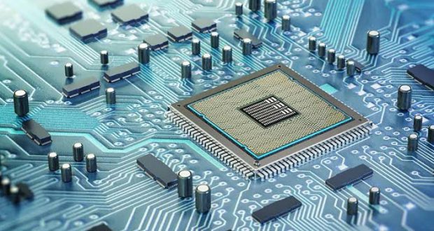
Odisha is aggressively rewriting its economic destiny. The transformation from a traditional resource economy into a sophisticated technological powerhouse represents a paradigm shift that will redefine India’s electronics landscape for generations.
Odisha is rapidly positioning itself as the premier semiconductor hub of eastern India, transitioning from a historical “mine economy” to a high-tech “mind economy”. Long celebrated for its rich natural resources, the state has orchestrated a calculated shift into technology, hardware manufacturing, and chip design. This momentum was fully on display at the high-profile SEMICON India 2026 conclave held in New Delhi, where the state emerged as a breakout destination for global chipmakers, technology innovators, and international investors. Under the leadership of Chief Minister Mohan Charan Majhi, the state government utilized the platform to pitch its robust infrastructure, progressive policies, and highly strategic vision to global players from Sweden, Taiwan, and Japan. The impact was immediate, with Odisha securing massive investment proposals worth approximately Rs 23,600 crore at the event, which are poised to generate thousands of direct and indirect employment opportunities.
Driven by unmatched policy incentives, a dedicated land bank at the Naraj Silicon Valley, and a rapidly evolving talent pool, Odisha is aggressively rewriting its economic destiny. The transformation from a traditional resource economy into a sophisticated technological powerhouse represents a paradigm shift that will redefine India’s electronics landscape for generations. By securing massive investment pipelines, introducing cutting-edge 3D glass packaging technologies, and pioneering advanced compound semiconductor fabrication, the state has clearly demonstrated that its ambitions are backed by concrete action and strategic execution. As the global electronics supply chain actively seeks resilience, stability, and innovation, this eastern powerhouse stands ready with the ideal mix of infrastructure and vision. Odisha has firmly broken away from the statuesque, decisively bridging the gap between raw natural wealth and high-tech manufacturing to solidify its position as the defining catalyst of India’s semiconductor future.
The defining announcement at the conclave was the unveiling of the Odisha Silicon Valley, a massive 870-acre technology enclave situated at Naraj near Cuttack. This integrated zone is architected to host top-tier semiconductor fabrication, advanced electronics system design and manufacturing, and major IT projects. Strategically aligned with the Cuttack-Bhubaneswar urban corridor, the Naraj site boasts efficient multimodal connectivity to deep-water maritime assets like the Paradip and Dhamara ports, alongside direct links to national highway networks. Crucially for the semiconductor industry, which relies on a constant and reliable resource base, the location next to the Mahanadi River secures the extensive water supply required for fabrication and chip assembly. Beyond the physical parameters of the site, this hub represents a concentrated effort to bring together the entire semiconductor supply chain, encompassing logistics, industrial gas units, chemical suppliers, and fabless design start-ups.
Odisha’s proactive industrial framework is anchored by the India Semiconductor Mission, commonly known as ISM. Recognizing the high-capital demands of the microchip industry, the state has actively aligned its state-level policies with the central government’s newly enacted Semicon 2.0 framework, which carries a national outlay of Rs 1,27,500 crore. Through its aggressive third policy amendment passed by the state cabinet, Odisha now offers an additional 25 percent capital expenditure support over and above the financial incentives provided by the central government. This supplementary fiscal cushion applies explicitly to projects involving semiconductor fabrication, advanced packaging, assembly testing, and critical supply chain elements like semiconductor-grade chemicals, raw materials, and specialised industrial gases. Additionally, the policy integrates operational sweeteners such as a ten-year electricity duty exemption, heavily subsidized power tariffs, rental assistance, and comprehensive support for international patent filings and commercial research and development.
This regulatory environment has already translated into concrete, ground-level execution, separating Odisha from states that rely strictly on speculative intent. Five major semiconductor projects are currently under construction within the state pipeline, representing an initial fixed investment of Rs 10,899 crore. Among these, two highly sophisticated projects approved by the Union Cabinet are being set up at the Info Valley complex in Khordha district near Bhubaneswar. The first is a Rs 2,066 crore commercial compound semiconductor fabrication unit being set up by SiCSem Private Limited. Rather than processing standard consumer computer chips, this facility is designed to manufacture Silicon Carbide diodes and MOSFETs. These components are crucial for specialized, heavy-duty electronics, electric vehicles, renewable energy systems, high-speed rail networks, and defence systems. The SiCSem facility alone is planned for an annual capacity of 60,000 wafers paired with a massive packaging capability. The second anchor project is a Rs 1,943 crore vertically integrated 3D Glass semiconductor packaging unit backed by prominent global technology firms including Intel and Lockheed Martin. This facility marks a massive leap forward for India, introducing cutting-edge 3D packaging technologies and embedded glass substrates that dictate the performance of next-generation telecommunications and advanced computing infrastructure.
Furthermore, the momentum generated at the conclave yielded immediate forward integration. The Odisha government signed a vital Letter of Intent with QuadQuantum to build a dedicated semiconductor facility focused on the production of Silicon Carbide substrate wafers. This addition addresses one of the most glaring vulnerabilities in the electronics production lifecycle: raw substrate material sourcing. By localizing wafer production alongside fabrication and advanced packaging plants, Odisha is positioning itself as a vertically integrated ecosystem where products can be developed entirely from raw materials to final assembled systems. Commercial electronics production is slated to begin rapidly, with a dedicated 20,000-square-foot production unit in Info Valley scheduled to go live. Beyond manufacturing, digital foundations are being simultaneously reinforced through new regional data centres planned in Koraput and Keonjhar, while a subsea cable landing station in Puri ensures high-bandwidth international data connectivity.
A sustainable technology ecosystem requires more than factories and fiscal handouts; it mandates a constant influx of highly trained human capital. The state is tackling this challenge through deep integration between its academic institutions and industrial requirements. During the conclave, the government highlighted a Rs 452 crore integrated power electronics hub established at IIT Bhubaneswar, which includes a specialized Rs 64 crore Research and Innovation Centre dedicated exclusively to Silicon Carbide technology. The state Government will continue Rs 125 crores for the project. This centre bridges the gap between laboratory research and commercial application, keeping the state at the cutting edge of material sciences. Simultaneously, institutional programs at NIT Rourkela and PMEC Berhampur are cultivating specialized engineering cadres in fabless chip design, electronic system automation, and device modelling. Specialized skilling hubs are being deployed across Khurda, Ganjam, and Rourkela to provide high-demand certifications in chip design and electronics manufacturing services, ensuring that engineering students from all parts of the state can build global technology careers locally. The semiconductor policy supports this human capital strategy by offering financial assistance for engineer relocation, corporate internships, and targeted manpower upskilling subsidies.
The broader macroeconomic goal of the state is to capture a significant portion of the global technology supply chain, encouraging a cluster-based industrial architecture. The approach emphasizes that individual projects must not be viewed in isolation; rather, anchor investments are intentionally used to draw a surrounding matrix of ancillary suppliers, assembly lines, and design startups. The state’s pavilion at the conclave, themed “Sand to Silicon,” highlighted this precise layout, demonstrating how its baseline industrial capabilities are evolving into complex technology frameworks. With thirty distinct IT and electronics projects currently moving through the pipeline, the state anticipates the generation of over 34,000 technology-focused jobs in the coming years. By combining unmatched fiscal capital support, a pre-certified land bank, an expanding skill pipeline, and an explicit focus on high-margin sectors like compound semiconductors and advanced 3D packaging, Odisha is fast becoming an essential powerhouse in India’s domestic semiconductor revolution.