India is breaking ground on its first advanced glass chip packaging unit in Odisha hoping to be the global leader by 2028-2030. Odisha is proud of establishing such advanced electronics manufacturing project with a vision to place itself in global map.
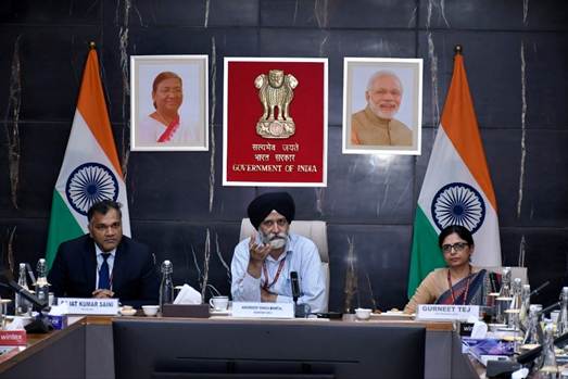
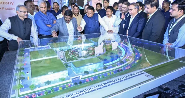
Hon’ble Mohan Charan Majhi, Chief Minister of Odisha laid the foundation stone for a 3-D glass chip packaging unit at Info valley in Bhubaneswar on 19th April 26 in presence of Union Electronics and IT Minister, Hon’ble Aswini Vaishnav in presence of Babu Mandava, President and CEO of 3D Glass Solutions, the promoter of the unit. The CEO of Intel Corp also joined the programme virtually from USA. This unit is one of the four semiconductor projects recently approved by Government of India, under India Semiconductor Mission (ISM) in August, 2025.
India Semiconductor Mission (ISM) acts as the nodal agency for the ‘Semicon India Program’ facilitating partnerships between government, industry and academia. It is a specialised division within Digital India Corporation which aims at creating a favourable ecosystem for promoting manufacturing, testing and packaging of semiconductor fabs, display fabs and compound semiconductors. The mission has an outlay of Rs 76,000 crore and it provides 50% fiscal support for manufacturing above high technology products. Till now, over 10 projects were approved by the mission with an outlay of Rs 1.60 lakh crore with two major packaging projects one each at Gujrat and Odisha. The main objective of the mission is to achieve 70-75% self-sufficiency in domestic chip demand by 2029. This Odisha project which was inaugurated recently has a proposed outlay of Rs1943 crore to produce next-generation chip packaging solutions.
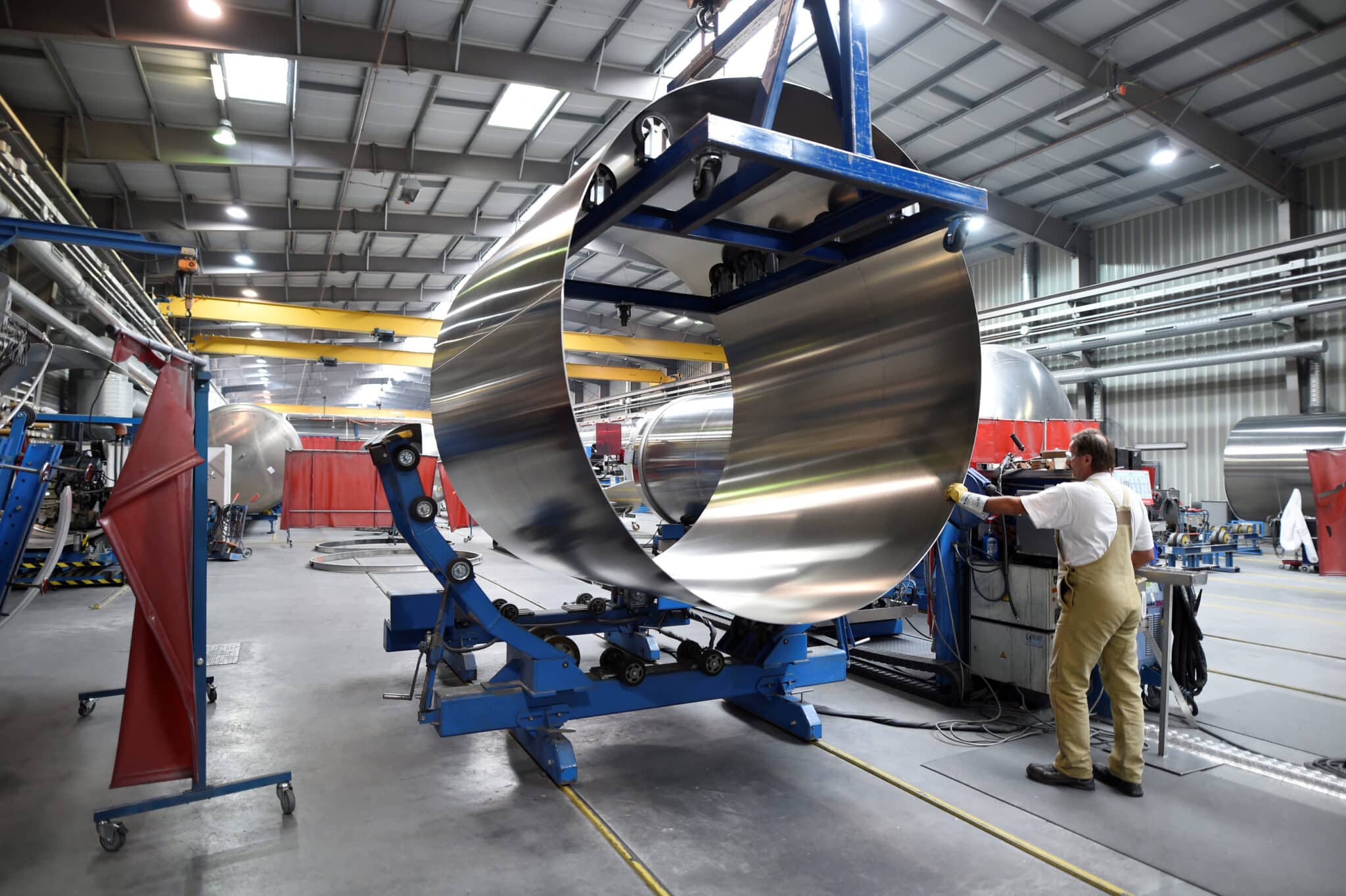
A material which conducts electricity is called a conductor and a substance that cannot conduct electricity is known as insulator. A semiconductor is a material with electrical conductivity between a conductor and an insulator. In simple terms, a semiconductor is an interconnected switch that can be turned on or turned off by electricity. Semiconductors are used for making micro-chips and processors (for computers and smartphones), transistors (as switches in electrical circuit), Diodes and LEDs (to control current direction and emit light), solar cells (converting light to electricity) and sensors (in devices, automobiles and industrial equipment). Silicon is the most widely used material in producing semiconductors.
The newly inaugurated advanced 3D glass chip packaging unit at Info valley in Bhubaneswar is projected to produce 70,000 glass panels annually along with 50 million assembled units and around 13,000 advanced 3DHI modules. This project will generate more than 2500 direct and indirect jobs in the areas if analytical computing, internet of Things (IOT) and artificial intelligence apart from areas of normal competencies.
According to Babu Mandava, President and CEO of 3D Glass Solutions, the company specialises in glass-based radio frequency and millimetre wave packaging substrates and the company, in Bhubaneswar facility, will build large substrates with advanced technology. Glass-based radio frequency (RF) in semiconductors uses specialised glass substrates, such as glass cores and interposers replacing traditional organic laminates thereby offering super frequency performance with low signal loss which is ideal for application in 5G, 6G and RADAR. In recent time, companies like SAM Tech, 3D Glass Solutions and SCHOTT are seen active in advancing glass-based RF solution.
Industry trend and future outlook of glass substrates based semi-conductor seems highly positive and ambitious. Major industry players like Intel, Samsung Electro-Mechanics, Absolics and SCHOTT are investing heavily in glass-core substrates for commercial production before 2030. The market for glass-based semiconductor is projected to grow at a CAGR 14% and reach US$ 4.4 billion by 2036. India is breaking ground on its first advanced glass chip packaging unit in Odisha hoping to be the global leader by 2028-2030. Odisha is proud of establishing such advanced electronics manufacturing project with a vision to place itself in global map.